In the world of high-speed electronics, even the smallest signal distortion or power fluctuation can impact performance. As devices become faster and more complex, engineers face new challenges in maintaining signal and power integrity. From the early days of simple PCB layouts to today’s multi-layer high-frequency boards, the evolution of these practices tells a story of innovation, precision, and necessity.
The Early Challenges of Signal & Power Integrity
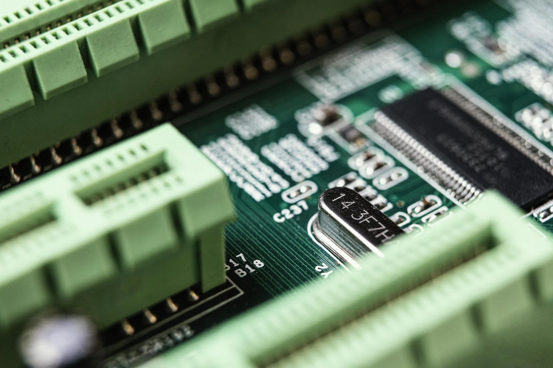
In the past, printed circuit boards (PCBs) operated at relatively low speeds. Designers didn’t have to worry much about signal degradation or power fluctuations because timing margins were large, and current demands were minimal.
However, as clock speeds increased and circuits became more compact, new issues began to surface:
- Crosstalk: High-speed signals started interfering with adjacent traces.
- Reflections: Poor impedance matching caused unwanted signal echoes.
- Electromagnetic Interference (EMI): Faster switching speeds led to excessive noise.
- Power fluctuations: Voltage drops and noise in the power delivery network (PDN) became critical concerns.
At this stage, manual routing techniques and basic design rules were the norm. But with the rise of high-speed systems, those methods were no longer enough.
How High-Speed Systems Changed the Game
Modern technologies like 5G, IoT, data centers, and automotive electronics demand faster data transfer, lower latency, and higher power efficiency. This shift dramatically raised the importance of signal and power integrity in PCB design.
Key changes include:
- Reduced timing margins: High-speed designs require precise control of trace length and impedance.
- Higher power density: Complex systems demand more robust PDNs.
- Stricter compliance requirements: Standards like PCIe, DDR, and USB-C pushed designers toward more advanced integrity solutions.
In today’s high-speed landscape, PCB signal integrity and power integrity design are no longer optional—they are core pillars of successful product development.
Key Factors Driving the Evolution
1. Advanced Simulation Tools
Modern simulation tools allow engineers to analyze and fix signal and power integrity problems before fabrication. These tools can:
- Predict crosstalk and reflections.
- Simulate PDN performance.
- Validate designs against compliance requirements.
Software like HyperLynx, Cadence Sigrity, and Ansys SIwave have become essential for high-speed PCB development.
2. Better PCB Materials
The materials used in PCB fabrication play a huge role in maintaining integrity. Low-loss laminates and high-frequency substrates significantly reduce signal attenuation, making them ideal for high-speed designs.
Common material upgrades include:
- Rogers laminates for RF designs.
- High-Tg FR4 for improved thermal and electrical performance.
- Low Dk/Df materials for better impedance control.
3. Integration of Power Integrity in Early Design
Power delivery is no longer an afterthought. Engineers now integrate PDN design into the earliest phases of PCB layout.
Key strategies include:
- Strategic decoupling capacitor placement.
- Plane partitioning to isolate noisy circuits.
- Optimized via placement to reduce impedance spikes.
This shift ensures that power remains stable across all components, even in the most demanding high-speed applications.
Modern Best Practices for Signal & Power Integrity
To ensure reliable performance, engineers must follow these core practices:
- Controlled impedance routing: Helps maintain signal quality across high-speed traces.
- Proper grounding and shielding: Minimizes EMI and crosstalk.
- Length matching and differential pair routing: Ensures timing alignment for high-speed signals like DDR and USB.
- Decoupling capacitor optimization: Stabilizes power delivery and reduces noise.
- Comprehensive SI/PI simulation: Detects and resolves integrity issues before production.
The Future of Signal & Power Integrity
As high-speed systems continue to evolve, so will signal and power integrity practices. Emerging trends include:
- AI-driven design tools: Predict and automatically fix integrity issues during layout.
- Real-time SI/PI feedback: Directly integrated into PCB CAD software.
- Next-generation PCB materials: Designed specifically for ultra-high-speed data rates.
- Improved power delivery models: For more complex multi-rail designs.
These advancements will allow engineers to create faster, more reliable systems while reducing time to market.
Final Thoughts
The evolution of signal and power integrity reflects the growing complexity of modern electronics. What was once a secondary consideration is now a critical factor for high-speed system success.
By leveraging advanced tools, selecting the right materials, and adopting best practices, engineers can design PCBs that deliver consistent performance in even the most demanding environments.
If your goal is to build reliable high-speed systems, it’s time to prioritize signal and power integrity—and work with experts who understand how to get it right the first time.
FAQ
Q1: What is the difference between signal integrity and power integrity?
Signal integrity focuses on preserving signal quality, while power integrity ensures stable voltage delivery to all components.
Q2: Why is simulation important for signal and power integrity?
Simulation tools help detect and resolve issues early, reducing costly redesigns and improving product reliability.
Q3: Can poor power integrity affect signal integrity?
Yes. Noise or instability in the power network can lead to timing errors, jitter, and signal degradation.