When it comes to the world of printed circuit boards (PCBs), castellated PCBs are becoming a popular choice for a wide range of applications. These specialized PCBs are distinguished by their unique feature: small, circular or oval holes along the edges, allowing for easy mounting of the PCB onto another board or surface. This comprehensive guide will explore everything you need to know about castellated PCB manufacturing, including their design, applications, and the key factors involved in the process. Additionally, we’ll delve into how companies like PCB Runner leverage advanced techniques to deliver high-quality castellated PCBs.
What Are Castellated PCBs?
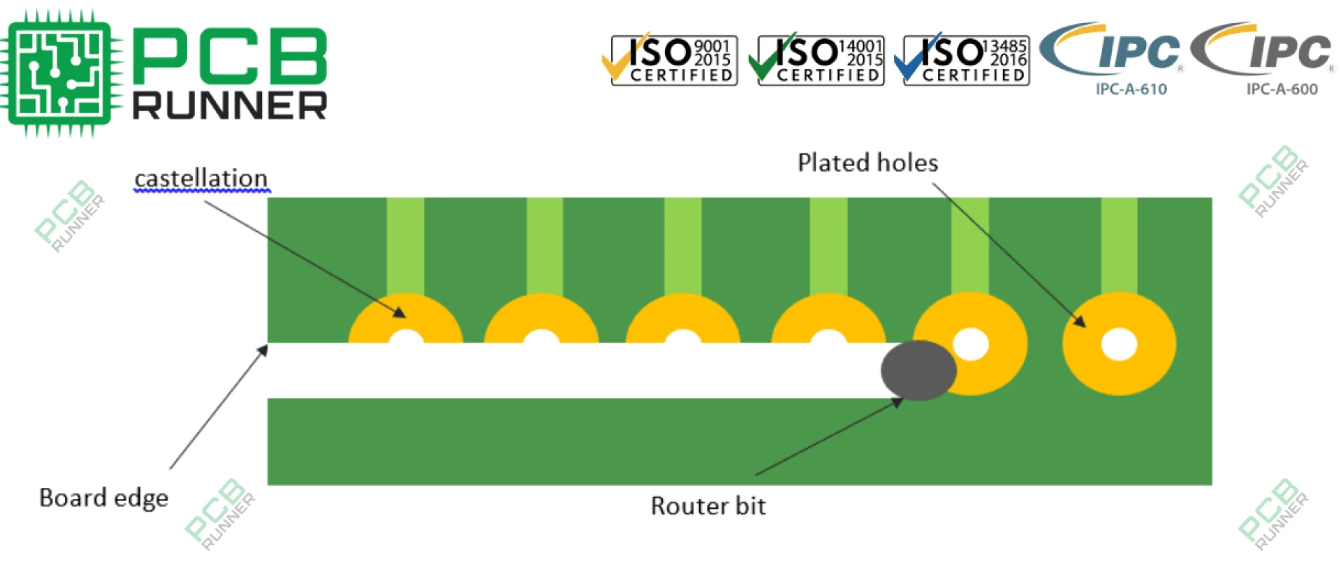
Castellated PCBs are designed with semi-circular or oval holes that are etched into the edges of the PCB. These holes are usually filled with solder and are intended for easy connection to another PCB or a component. The term “castellated” is derived from the word “castle,” referring to the shape of the holes, which resemble battlements or crenellations found in castle walls.
These PCBs are crucial for applications that require quick assembly, easy reworkability, or compact designs where space is limited. Castellated PCBs allow for a more efficient interconnection of different circuit boards or components without the need for complex connectors or other mounting solutions.

Understanding the Benefits of Castellated PCBs
There are several advantages of choosing a castellated PCB for your design:
- Reduced Size and Complexity
- Castellated PCBs are typically smaller than traditional PCBs and can be designed to fit into more compact enclosures. The use of castellated holes reduces the need for extra connectors, which can simplify the overall design and improve the layout's efficiency.
- Easy Soldering and Rework
- The holes in a castellated PCB provide a direct path for soldering. This simplifies the soldering process, which can be especially useful when assembling multiple boards. If any issues arise, rework is straightforward since the PCB can be easily desoldered and reattached without much complexity.
- Cost-Effective
- The efficient design and straightforward manufacturing process of castellated PCBs can reduce production costs compared to other PCB types. The reduced need for additional components and connectors helps lower both material and labor costs.
- Improved Durability and Stability
- Castellated PCBs offer superior mechanical stability, particularly in applications where the board will undergo vibrations or stress. The direct connection via the castellated holes ensures that the PCB is securely attached, reducing the risk of disconnections or damage over time.
The Process of Castellated PCB Manufacturing
The manufacturing process of castellated PCBs is quite similar to that of standard PCBs, with the addition of special steps to create the castellated holes. Here's an overview of how the process typically works:
1. Design and Layout
The first step is designing the PCB using specialized software. A key part of the design is deciding where to place the castellated holes along the edges of the PCB. Designers must consider the size, spacing, and number of holes required for the intended application. This is where castellated PCB design plays a significant role, as it determines how the holes will interact with the surrounding components and boards.
2.Fabrication
After the design is complete, the PCB goes through the fabrication process. This includes etching the copper traces, applying the solder mask, and adding any necessary components. The edges of the PCB are carefully prepared for the castellated holes, which are drilled and plated to ensure they are conductive and ready for soldering.
3.Drilling the Castellated Holes
The unique feature of castellated PCBs is the drilling of holes along the edge. These holes are typically drilled in a manner that only partially cuts through the PCB. This allows the holes to remain as part of the board but still provide a mounting point for connections to other surfaces. The drilling is a critical part of the process, as it requires precision to ensure the holes align perfectly for smooth assembly.
4.Plating and Soldering
Once the holes are drilled, they are plated with copper to ensure electrical conductivity. The plating process can also help improve the overall durability of the PCB. After plating, the PCB undergoes a soldering process where the holes are filled with solder, ready for connection to another PCB or component.
5.Testing and Inspection
The final step involves testing and inspecting the PCB to ensure it meets all electrical and mechanical requirements. This may include visual inspections, electrical testing, and mechanical stress testing. At PCB Runner, advanced testing equipment is used to verify the quality and performance of each PCB before it is shipped.
Applications of Castellated PCBs
Castellated PCBs are used in a wide variety of applications, from consumer electronics to industrial machinery. Some common uses include:
- Modular Electronics: Castellated PCBs allow for easy assembly and disassembly, making them ideal for modular electronics that may need to be reconfigured or repaired frequently.
- Wearable Devices: Due to their compact design and efficient manufacturing process, castellated PCBs are often found in wearable devices, where space is at a premium.
- Prototyping and Development: The ease of soldering and reworking castellated PCBs makes them a popular choice for prototyping new products and testing designs before finalizing the production process.
- Medical Devices: The durability and reliability of castellated PCBs make them suitable for medical equipment, where high performance and small form factors are essential.
Challenges in Castellated PCB Design
While castellated PCBs offer numerous benefits, designing them comes with its own set of challenges. Some common issues include:
- Alignment Issues: Ensuring that the castellated holes align correctly with the mating board or component can be challenging. Any misalignment can lead to poor connections or performance issues.
- Plating and Drilling Precision: The precision required to drill the holes and apply the plating is critical to the overall success of the design. Inaccuracies in this process can affect the functionality of the PCB.
- Thermal Management: The compact nature of castellated PCBs can sometimes lead to heat buildup, particularly in high-power applications. Proper thermal management techniques must be employed to ensure the PCB operates within safe temperature ranges.
Conclusion
Castellated PCBs are an essential part of modern electronics, offering a practical and efficient solution for various applications. Whether you're designing a modular system, wearable technology, or a medical device, understanding the intricacies of castellated PCB design can significantly enhance the performance and durability of your product. Manufacturers like PCB Runner specialize in delivering high-quality castellated PCBs that meet the highest standards of precision, reliability, and performance.
As the demand for smaller, more efficient designs continues to grow, castellated PCBs will remain an essential technology for engineers and designers worldwide. By considering all the factors involved in the manufacturing process, you can ensure that your castellated PCBs are up to the task, enabling your product to succeed in a competitive market.