

The semiconductor industry is entering an era in which performance gains are increasingly being achieved not only through smaller process nodes, but also through advanced packaging and heterogeneous integration. System-in-Package (SiP) technology has emerged as a critical solution, enabling multiple semiconductor dies and functional components, including processors, memory, sensors, RF modules, and power management ICs, to operate within a single compact package.
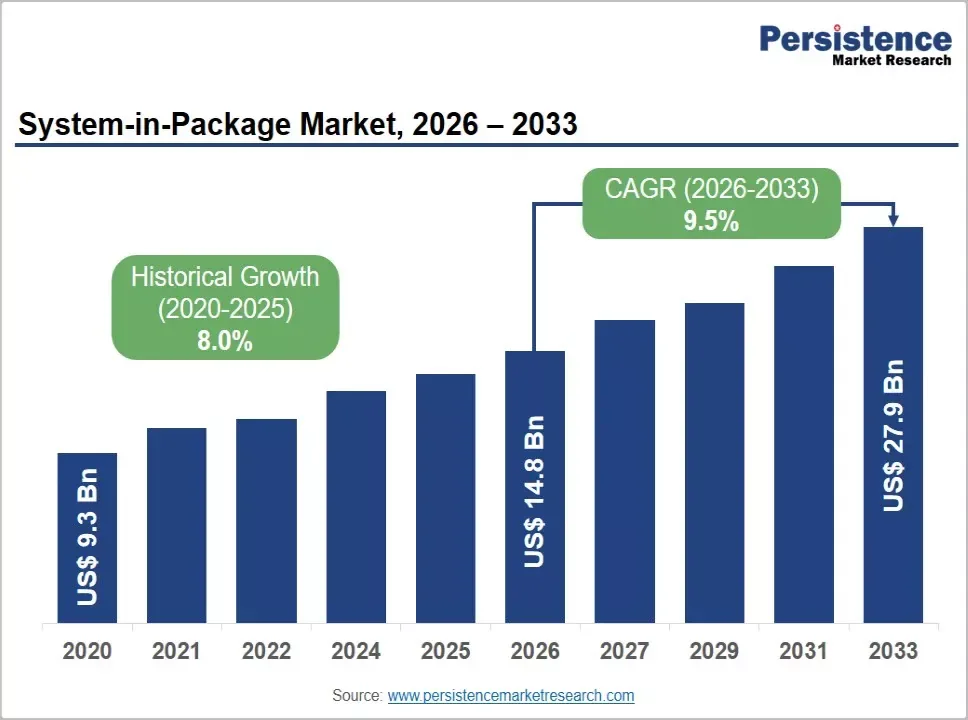
The global System-in-Package market is expected to reach US$14.8 billion in 2026 and is projected to grow to US$27.9 billion by 2033, registering a CAGR of 9.5% during the forecast period. This expansion is being supported by the rapid deployment of 5G networks, growing AI workloads, increasing semiconductor content in vehicles, the proliferation of connected devices, and rising demand for smaller and more power-efficient electronics.
Unlike conventional packaging approaches that primarily protect and connect an individual chip, SiP allows designers to combine heterogeneous components into one integrated solution. This reduces interconnect distances, saves board space, improves power efficiency, and can accelerate product development.
The importance of advanced packaging is particularly visible in high-performance computing. TSMC's 2025 Annual Report highlighted that advanced technologies represented 74% of its total wafer revenue in 2025, while the company continued expanding CoWoS, InFO, and SoIC capacity to address increasing demand from AI and high-performance computing customers.
What Is Driving the System-in-Package Market?
The fundamental attraction of SiP is its ability to deliver greater functionality within increasingly constrained physical dimensions. As electronic products become smarter and more connected, manufacturers need to integrate more capabilities without proportionally increasing device size.
SiP addresses this requirement by combining multiple components into a unified package. Depending on the application, a single SiP can integrate a processor, memory, RF circuitry, sensors, connectivity components, and power management functions.
This architecture is particularly valuable for smartphones, smartwatches, hearables, IoT devices, networking equipment, automotive electronics, and AI-enabled edge devices.
5G Expansion Accelerates Demand for RF SiP Modules
The global expansion of 5G networks is one of the strongest demand generators for SiP technology. Modern wireless devices require increasingly sophisticated RF front-end architectures incorporating power amplifiers, filters, duplexers, low-noise amplifiers, antenna switches, and other components.
Integrating these components into compact SiP modules can reduce signal loss and improve electrical performance while saving valuable board space.
According to the Ericsson Mobility Report 2025, global 5G subscriptions reached approximately 2.9 billion at the end of 2025 and are projected to exceed 6.3 billion by 2030. As 5G adoption expands across smartphones, fixed wireless access, industrial networks, and small-cell infrastructure, demand for highly integrated RF modules is expected to rise.
Companies such as Murata Manufacturing, Skyworks Solutions, and Qorvo are strengthening their RF module capabilities to serve these applications.
AI and Edge Computing Transform Semiconductor Packaging
Artificial intelligence is also changing the economics and architecture of semiconductor packaging. AI workloads require high bandwidth, low latency, efficient power delivery, and increasingly sophisticated combinations of logic and memory.
At the edge, AI-enabled smartphones, PCs, wearables, cameras, industrial equipment, and automotive systems require powerful processing capabilities without the size and energy penalties associated with conventional discrete architectures.
SiP allows processors, memory, connectivity, and power-management components to be integrated into compact modules. Shorter interconnects can help reduce latency and power consumption while improving system-level performance.
Companies such as Qualcomm, Apple, and MediaTek are investing heavily in architectures designed for AI-enabled consumer and edge applications, supporting long-term demand for heterogeneous integration.
Advanced Packaging Technologies Reshape the Market
The System-in-Package market is evolving rapidly as semiconductor manufacturers adopt 2.5D and 3D integration to address the limitations of traditional planar architectures.
2.5D IC Remains the Leading Technology
2.5D IC is expected to account for more than 48% of the global SiP market in 2026, representing more than US$7.1 billion in value.
The technology has become especially important for AI accelerators, high-performance computing platforms, networking processors, and applications requiring high-bandwidth memory.
2.5D architectures typically place multiple dies alongside each other on an interposer, allowing high-density communication between logic and memory components. This architecture is particularly attractive for AI processors because it supports high-bandwidth communication with HBM while maintaining relatively compact package dimensions.
TSMC's CoWoS platform has become an important example of this approach. Continued demand for AI processors has encouraged significant investment in additional advanced packaging capacity.
3D IC Represents the Fastest-Growing Technology
While 2.5D currently leads the market, 3D IC is expected to record the fastest growth during the forecast period.
3D integration stacks semiconductor dies vertically, potentially reducing interconnect distances and increasing functional density. Through-silicon vias and other advanced interconnect technologies allow signals to move between stacked dies efficiently.
This approach is increasingly relevant to AI processors, memory technologies, and applications where conventional scaling cannot deliver sufficient performance within available space and power constraints.
The development of high-bandwidth memory is also demonstrating the commercial potential of vertical integration. SK hynix's work on advanced HBM architectures illustrates how vertically stacked memory is becoming increasingly important for AI infrastructure.
Flip Chip Leads, While Fan-Out Gains Momentum
Packaging methods are another important dimension of SiP market development.
Flip Chip is expected to capture more than 52% of the market in 2026, representing over US$7.7 billion.
The technology provides high I/O density, strong electrical performance, and reduced signal path length. These characteristics make it suitable for processors, RF components, networking equipment, AI hardware, and other performance-sensitive applications.
Flip-chip packaging is particularly valuable as semiconductor devices operate at increasingly high frequencies and require more connections within limited package areas.
At the same time, Fan-out Wafer-Level Packaging (FOWLP) is the fastest-growing packaging method.
FOWLP eliminates the need for some conventional substrate requirements and can enable thinner packages with improved electrical characteristics. These benefits are particularly attractive in smartphones, smartwatches, wireless devices, and edge AI products where package thickness and power consumption are important design considerations.
Consumer Electronics Remains the Largest End-Use Market
Consumer electronics is expected to remain the largest end-use industry, accounting for more than 36% of the global SiP market in 2026, equivalent to more than US$5.3 billion.
Smartphones, tablets, smartwatches, wireless earbuds, and other connected devices require increasingly sophisticated electronics within extremely small form factors.
A smartwatch, for example, may need to integrate a processor, memory, wireless connectivity, sensors, power management, and other components while maintaining a compact physical footprint. SiP makes this level of integration possible.
Apple's use of SiP architectures in its Apple Watch product family demonstrates how advanced packaging can become a fundamental part of consumer product design rather than simply a back-end manufacturing technology.
Automotive Becomes a High-Growth Opportunity
Automotive and transportation is expected to be the fastest-growing end-use industry for SiP.
Electric vehicles and advanced driver-assistance systems are dramatically increasing the amount of semiconductor content per vehicle. Cameras, radar, lidar, connectivity systems, domain controllers, battery-management systems, and power electronics all require compact and reliable semiconductor solutions.
SiP can combine processors, sensors, memory, connectivity, and power-management functions within integrated modules while supporting demanding automotive operating environments.
The International Energy Agency reported that global electric vehicle sales exceeded 20 million units in 2025, representing more than one-quarter of new passenger vehicle sales worldwide. Continued EV adoption is therefore likely to create additional opportunities for automotive-grade SiP technologies.
Wearables and Healthcare Create New Opportunities
Wearable healthcare is another promising application area. Smartwatches, fitness trackers, hearables, and medical monitoring devices increasingly incorporate sophisticated sensors and processing capabilities.
A health-focused SiP may integrate biosensors, analog front-end circuitry, wireless connectivity, processors, and power management within a highly compact package.
This integration is particularly important for wearable devices because consumers expect products to become smaller and lighter while offering more functionality.
The wearable device market provides a strong foundation for this trend. Global wearable device shipments exceeded 143 million units in the first quarter of 2026, while hearables are projected to exceed 400 million units during 2026.
As continuous health monitoring expands, ultra-miniaturized SiP architectures could become increasingly important in glucose monitoring, cardiac monitoring, fitness tracking, and other connected healthcare applications.
High Costs and Yield Challenges Remain Major Restraints
Despite its advantages, SiP adoption is not without challenges.
One of the largest barriers is the high cost associated with designing and manufacturing complex multi-die packages. SiP requires close coordination between semiconductor design, package engineering, substrate design, thermal management, and reliability testing.
For low-volume products, these development costs can be difficult to justify.
Another challenge is yield management. A SiP may contain several dies produced using different process technologies and potentially sourced from different manufacturing facilities. A defect in any critical component can compromise the final package.
Consequently, manufacturers must carefully manage known-good-die availability, traceability, testing, and assembly processes.
Industry initiatives such as the UCIe Consortium and ongoing JEDEC standardization are helping address interoperability and chiplet integration challenges. Broader standardization could ultimately reduce barriers to multi-die system design.
Asia Pacific Maintains Global Leadership
Asia Pacific is expected to account for more than 55% of the global SiP market in 2026, representing more than US$8.1 billion.
The region's dominance reflects its integrated semiconductor ecosystem spanning foundries, OSAT providers, advanced packaging facilities, memory manufacturers, and consumer electronics companies.
Taiwan remains particularly important because of TSMC's advanced packaging capabilities, including CoWoS, InFO, and SoIC. ASE Technology Holding is also a major force in high-volume advanced packaging.
China is expected to generate more than US$4.48 billion in SiP market value in 2026, supported by expanding domestic semiconductor and packaging capabilities.
South Korea is another major center, with Samsung Electronics and SK hynix investing in advanced memory and heterogeneous integration technologies.
Japan contributes through companies such as Shinko Electric Industries and KYOCERA, while Southeast Asian markets including Malaysia and Vietnam are strengthening their assembly and testing capabilities.
India is also emerging as an important semiconductor packaging location, supported by the India Semiconductor Mission and investments from companies such as Micron Technology and Tata Electronics.
North America Focuses on Advanced Packaging Innovation
North America is expected to account for more than 22% of the global SiP market in 2026, reaching approximately US$3.26 billion.
The region's strength is rooted in semiconductor design leadership. NVIDIA, Intel, AMD, Qualcomm, Broadcom, and Marvell are developing increasingly sophisticated processors and chiplet-based architectures that depend on advanced packaging.
The United States is also attempting to strengthen domestic packaging capacity and reduce reliance on overseas manufacturing.
Amkor Technology's planned advanced packaging and test campus in Peoria, Arizona, represents a major investment in U.S. semiconductor infrastructure. The company announced a US$2 billion investment in the project, with production targeted for 2028.
Meanwhile, Intel's Foveros technology demonstrates how 3D packaging is becoming an important part of the company's processor roadmap.
Europe Builds a Strategic Packaging Ecosystem
Europe's SiP market is supported by the European Chips Act and the region's strong automotive and industrial semiconductor industries.
The European market is projected to reach approximately US$2.07 billion in 2026.
Germany remains an important market because of its automotive manufacturing base and semiconductor ecosystem. Infineon's investments in Dresden, along with semiconductor activities involving Bosch and other industrial players, are supporting the development of regional semiconductor capabilities.
France is also strengthening its semiconductor ecosystem through the France 2030 program, while the Netherlands, Belgium, Sweden, and Italy contribute through semiconductor equipment, research, telecommunications, and industrial electronics.
The broader European push toward semiconductor sovereignty is expected to increase interest in advanced packaging, particularly for automotive, industrial automation, telecommunications, and energy applications.
Competitive Landscape
The SiP market has a capability-driven competitive structure, with leading companies competing through packaging technology, manufacturing yield, substrate capabilities, thermal management, scalability, and reliability.
Key participants include ASE Technology Holding, Amkor Technology, TSMC, Samsung Electronics, Intel, JCET Group, Powertech Technology, SK hynix, Micron Technology, Shinko Electric Industries, KYOCERA, Unimicron Technology, Tongfu Microelectronics, and Huatian Technology.
Competition is increasingly shifting beyond traditional packaging services toward complete heterogeneous integration capabilities.
Companies that can successfully integrate advanced logic, HBM, chiplets, substrates, thermal solutions, and high-density interconnects will be better positioned to capture growth from AI and HPC applications.
Strategic partnerships are also becoming more important. In June 2026, TSMC and Amkor Technology announced a 10-year strategic partnership aimed at expanding advanced semiconductor packaging and testing capabilities in Arizona.
The Road Ahead for System-in-Package
The System-in-Package market is moving from a niche packaging solution toward a foundational technology for modern electronics.
The market's projected expansion from US$14.8 billion in 2026 to US$27.9 billion by 2033 reflects a broader transformation in semiconductor engineering. As transistor scaling becomes more expensive and technically challenging, advanced packaging provides another pathway to increase system performance.
The next phase of growth will be shaped by AI accelerators, HBM, chiplets, 5G, automotive electronics, wearables, edge computing, and connected devices. 2.5D will remain critical for high-bandwidth applications, while 3D integration and fan-out packaging are likely to gain momentum as manufacturers pursue greater performance and miniaturization.
At the same time, improvements in chiplet standards, known-good-die testing, package design automation, and advanced manufacturing processes could gradually reduce some of the complexity currently limiting adoption.
Ultimately, SiP is becoming much more than a packaging technology. It is evolving into an essential platform for bringing together heterogeneous semiconductor components and delivering the performance, efficiency, and compactness required by the next generation of AI, consumer, automotive, industrial, and communication systems.