

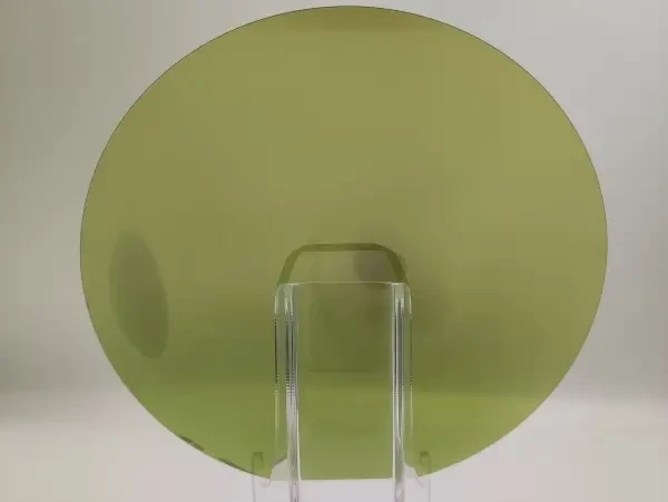
Silicon Carbide has proven its value as the core material for third-generation power semiconductors, critical for high-voltage, high-efficiency applications like Electric Vehicle  inverters and renewable energy systems. The current industry standard is the 6-inch ($\text{150mm}$) wafer, but the focus has emphatically shifted to the 8-inch ($\text{200mm}$) 4H-N Type SiC substrate as the pathway to mass-market affordability.
The question of whether 8-inch $\text{SiC}$ will fully replace 6-inch to become the mainstream is no longer if, but when, and depends entirely on the industry's ability to overcome specific technical and economic challenges in the coming years.
The Compelling Economic Argument for Scaling
The primary driver behind the move to 8-inch wafers is the proven concept of economies of scale. In semiconductor manufacturing, larger wafers dramatically reduce the manufacturing cost per chip (die).
- Area Increase: An 8-inch wafer offers approximately 78% more usable area than a 6-inch wafer.
- Die Output: This translates to a near doubling of the chip output per production batch.
- Cost Reduction: Experts calculate that transitioning from 6-inch to 8-inch can reduce the cost per unit device by an additional 35% to 50%.
Since the cost of the $\text{SiC}$ substrate often accounts for up to 50% of the total device cost, achieving this cost reduction is paramount for $\text{SiC}$ to reach cost-parity with mature silicon-based solutions and unlock widespread adoption across mass-market applications like
Technical Hurdles and the Road to Mainstream
While the economic incentive is clear, the transition faces major technological challenges, which dictate the timeline for 8-inch dominance:
1. Crystal Growth and Quality
Growing the large, high-quality $\text{SiC}$ single crystal boule is the biggest obstacle. The current growth method (Physical Vapor Transport or $\text{PVT}$) is inherently difficult due to the high temperatures and the material's hardness.
- Defect Density: Scaling to 8-inch increases the difficulty of maintaining a uniform thermal field, leading to higher levels of critical defects like micropipes and stacking faults that ruin device yield.
- Resistivity Uniformity: Achieving consistent electrical properties (resistivity) across the entire 8-inch surface is challenging, impacting the reliability of the final
2. Processing and Supply Chain Maturity
The entire ecosystem must adapt. While the 6-inch supply chain is mature, 8-inch production requires new, expensive equipment.
- New Tooling: Specialized slicing, grinding, polishing, and epitaxial tools must be validated and standardized for the 8-inch format.
- Metrology: Inspection tools need to be upgraded to accurately characterize defects and stress on the larger, semi-transparent surface.
Global Roadmap and Outlook
The industry consensus is strong: 8-inch will become the mainstream standard for power devices in the long term. Leading global players are aggressively investing in dedicated 8-inch fabs and driving technological breakthroughs.
PhaseTimeline (Est.)Status of 8-inch SiCRoleCurrent/Short Term1-2 Years Small-scale sampling, Customer qualificationStrategic ReserveMedium Term3-5 YearsYields improve, costs drop, major vendors start mass productionAccelerating Adoption (Especially in Automotive)Long Term5+ YearsBecomes the dominant wafer size for high-volume power devicesIndustry Mainstream
The global competition is now focused on improving crystal growth yields and standardizing 8-inch processes, which will determine how quickly this transition occurs.
For a deeper dive into the specific technological and market dynamics driving the shift from 6-inch to 8-inch substrates, including detailed analysis from industry experts, you can read the full blog post on this subject: JXT Wafer Blog Post (https://jxtwafer.com/about/blogs/1284.html).
In conclusion, the immense cost advantages and market demand from sectors like the industry make the mainstream adoption of 8-inch 4H-N Type substrates inevitable. The industry is actively building the infrastructure required to realize this goal, signaling a transformative phase for power electronics.
Visit the JXT Wafer Homepage: To explore the latest advancements in $\text{SiC}$ and other next-generation semiconductor materials that are shaping the future of power applications, please visit our main website: https://jxtwafer.com/.