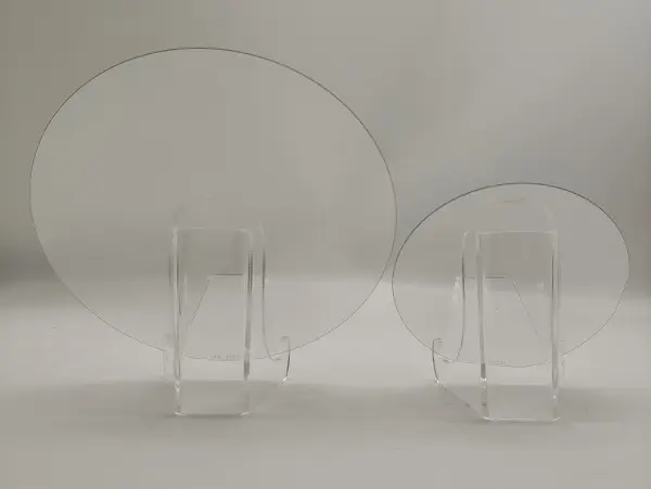
The shift to 8-inch (200mm) Silicon Carbide (SiC) substrates is widely heralded as the critical next step for reducing costs in the power semiconductor industry. Manufacturers are making rapid progress with 8-inch N-Type (conductive) SiC wafers, which are essential for electric vehicle (EV) inverters and power supplies.
However, a parallel but equally important material, the 8-inch Semi-Insulating (SI) SiC substrate, remains largely confined to the lab. Why is one size-expansion moving quickly while the other is stalled?
The answer lies in a combination of profound technical complexity and crucial market dynamics. Semi-Insulating SiC is the foundation for high-frequency and radio-frequency (RF) applications, particularly in 5G infrastructure, aerospace, and defense, which require exceptional performance characteristics that are exponentially harder to achieve at a larger diameter.
1. The Superior Material Growth Complexity
The primary difficulty is material science. While both N-Type and SI-Type are typically 4H-SiC, their requirements are vastly different:
- N-Type (Conductive): Focuses on uniform resistivity within a tight, low range to conduct electricity efficiently in power devices.
- SI-Type (Semi-Insulating): Requires an extremely high and uniform resistivity (low conductivity) to provide superior electrical isolation. This is typically achieved through complex doping (like Vanadium) or ultra-high-purity growth.
Expanding the SiC crystal from 6-inch to 8-inch already introduces challenges with thermal field control, crystal stress, and defect management. For SI-SiC, these issues are magnified. Any microscopic variation in the concentration of the compensation mechanism (dopants or defects) across the 8-inch wafer can lead to non-uniform resistivity or high leakage current, instantly rendering the expensive wafer unusable for sensitive RF applications. Controlling this purity and uniformity at the 8-inch scale pushes the limits of current crystal growth technology.
2. Market Focus and Economic Viability
Beyond the technical hurdles, the economic equation simply doesn't favor the 8-inch SI wafer—yet.
- The Power Device Driver: The Electric Vehicle market is driving unprecedented demand for SiC. This enormous volume of orders for power modules justifies the billions in investment necessary to overcome the 8-inch N-Type development challenges. The return on investment for 8-inch N-Type is clear and immediate.
- The RF Market Gap: The high-frequency RF market, while growing, is significantly smaller than the power device market. Manufacturers follow the money, prioritizing the development of the N-Type substrate where the immediate volume and profit are. The investment required to solve the far greater technical difficulty of 8-inch SI SiC is currently not justified by the short-term market size and volume demand.
The Future Outlook
The industry consensus is that 8-inch N-type substrates will soon become the mainstream for power devices. Semi-insulating SiC substrates will likely remain at the 6-inch diameter for the short-to-medium term. The transition to 8-inch SI will only occur once the technical challenges are conquered and the demand from 5G, 6G, and high-power RF applications grows to a scale that warrants the monumental capital and R&D expenditure.
For a detailed, professional breakdown of the complexities and timeline expectations regarding 8-inch Semi-Insulating SiC substrates, you can read the full analysis: Why There Are No 8 inch Semi-Insulating SiC Substrates Yet?