

Silicon Carbide ($\text{SiC}$) has solidified its position as the premier material for third-generation power semiconductors, rapidly replacing traditional silicon ($\text{Si}$) in high-power and high-efficiency applications. The transition from the current industry standard of 6-inch ($\text{150mm}$) wafers to the larger 8-inch ($\text{200mm}$) 4H-N Type SiC substrate is the single most important factor poised to unlock massive cost reductions and drive the widespread commercialization of $\text{SiC}$ devices. This strategic upgrade is critical for meeting the accelerating demand from key sectors like electric vehicles (EVs) and sustainable energy infrastructure.
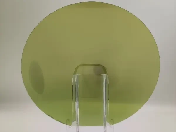
Understanding the Technology: 4H-N Type SiC
The specific material configuration, 4H-N Type SiC, is not arbitrary; it is chosen for optimal performance in power devices:
- 4H-SiC Polytype: This crystal structure offers superior physical properties, including the highest electron mobility and a high breakdown electric field strength compared to other $\text{SiC}$ polytypes (like 6H), making it the optimal choice for high-voltage, high-efficiency power devices such as $\text{MOSFETs}$ (Metal-Oxide-Semiconductor Field-Effect Transistors) and Schottky diodes.
- N-Type (Conductive) Substrate: The "N-Type" doping (electron-conductive) is essential for creating the low-resistance substrates required for the vast majority of power device architectures, which rely on vertical current flow for maximum efficiency and power density.
This combination forms the fundamental building block for the chips that power high-performance systems.
The Economic Imperative: Cost Reduction through Scaling
The primary driver for the move to 8-inch wafers is economics. Currently, the high cost of $\text{SiC}$ wafers represents a significant portion—often 45% to 65%—of the final power device cost, which slows adoption. Wafer diameter scaling is a proven strategy from the $\text{Si}$ industry to reduce the cost per chip ($\text{die}$) by leveraging economies of scale.
Parameter6-inch (150mm)8-inch (200mm)ImprovementWafer Area$\approx 176.7\text{ cm}^2$$\approx 314.2\text{ cm}^2$$\mathbf{\approx 78\%}$ more areaPotential Chip OutputBaseline$\approx 1.8 \times$ to $2.0 \times$Near doubling of chips per waferCost Per Die ReductionBaselineUp to 35% to 50% reductionSignificant cost advantage
While the cost of processing a larger wafer increases, the near-doubling of the usable area and a substantial increase in chip output far outweigh the incremental manufacturing expenses. This leap in efficiency is seen as crucial for enabling cost-parity with traditional silicon-based solutions in the long term, thereby accelerating mass market adoption.
Key Applications Driving 8-inch Adoption
The demand for larger, lower-cost $\text{SiC}$ wafers is being directly fuelled by high-growth, energy-intensive sectors:
Electric Vehicles ($\text{EVs}$)
$\text{SiC}$ power modules are essential in $\text{EV}$ powertrains, particularly in the traction inverter and the on-board charger ($\text{OBC}$). Using $\text{SiC}$ enables:
- Extended Driving Range: $\text{SiC}$ significantly reduces power losses in the inverter (up to $80\%$), which translates directly into better energy utilization and up to a $10\%$ longer driving range for the same battery size.
- Faster Charging: $\text{SiC}$ devices handle higher power and faster switching speeds, which is vital for efficient high-power fast-charging stations.
- Smaller, Lighter Systems: The material's ability to operate at higher temperatures and frequencies allows for smaller, lighter, and more compact electronic systems, which is a major advantage for vehicle design.
Renewable Energy and Energy Storage ☀️
In solar and wind power, $\text{SiC}$ enhances the efficiency and power density of inverters and converters. For large-scale energy storage systems, the low-loss characteristics of $\text{SiC}$ are critical for efficient power management and grid integration. As governments worldwide push for clean energy infrastructure, the demand for $\text{SiC}$ components is only set to grow.
The Technical Hurdles in Scaling Production
The move from 6-inch to 8-inch is not merely a matter of increasing size; it presents a complex array of technological challenges in the manufacturing process:
1. Crystal Growth and Defect Control
The vast majority of $\text{SiC}$ substrates are grown using the Physical Vapor Transport ($\text{PVT}$) or seeded sublimation technique at extremely high temperatures ($\approx 2500^\circ\text{C}$). Scaling the crystal boule size to 8-inch exacerbates existing material challenges:
- Increased Defect Density: Larger crystals are more prone to critical defects like micropipes, stacking faults, and dislocations (specifically Basal-Plane Dislocation, $\text{BPD}$), which dramatically reduce device yield and compromise long-term reliability.
- Thermal Uniformity: Maintaining a highly uniform temperature and gas-phase material distribution across a much larger growth furnace is significantly more difficult, leading to internal stress and potential crystal cracking or warpage.
2. Wafer Processing and Metrology
After the crystal is grown, turning it into a polished wafer and device requires specialized tools:
- Flatness and Warpage: $\text{SiC}$ wafers naturally exhibit more curvature and less flatness compared to $\text{Si}$. Scaling to 8-inch increases this issue, which complicates subsequent lithography and etching steps where precision is paramount.
- Tooling Gap: The entire ecosystem—including slicing, grinding, polishing, epitaxial growth equipment, and inspection tools—must be upgraded and certified for the 8-inch format. Since $\text{SiC}$ wafers are semi-transparent, standard silicon metrology tools are often incompatible, requiring $\text{SiC}$-specific solutions.
Market Landscape and Future Outlook
The industry consensus is that 8-inch 4H-N Type $\text{SiC}$ substrates will become the mainstream standard for power devices. Leading global manufacturers like Wolfspeed, STMicroelectronics, and ON Semiconductor are heavily investing in 8-inch fabrication facilities ($\text{fabs}$), with many planning to begin mass production and qualification around 2025.
Phased Transition Timeline 🚀
- Short Term (Current): $\text{6-inch}$ wafers remain dominant. $\text{8-inch}$ is in the $\text{R}\&\text{D}$, sampling, and customer qualification stage.
- Medium Term ($\mathbf{3-5}$ years): As manufacturing yields improve and technical challenges are resolved, $\text{8-inch}$ substrates will begin to scale into high-volume applications, particularly in the automotive sector.
- Long Term ($\mathbf{5+}$ years): $\text{8-inch}$ is projected to become the primary industry standard, fundamentally reshaping the cost structure of power electronics and accelerating the global shift towards more energy-efficient technologies.
This ongoing transition represents a critical technology battleground, where success hinges on achieving both high yield and high quality for these larger, more complex wafers. To learn more about the future of $\text{SiC}$ and other semiconductor materials, and to see examples of these advanced products, visit the dedicated homepage at JXT Wafer (https://jxtwafer.com/).