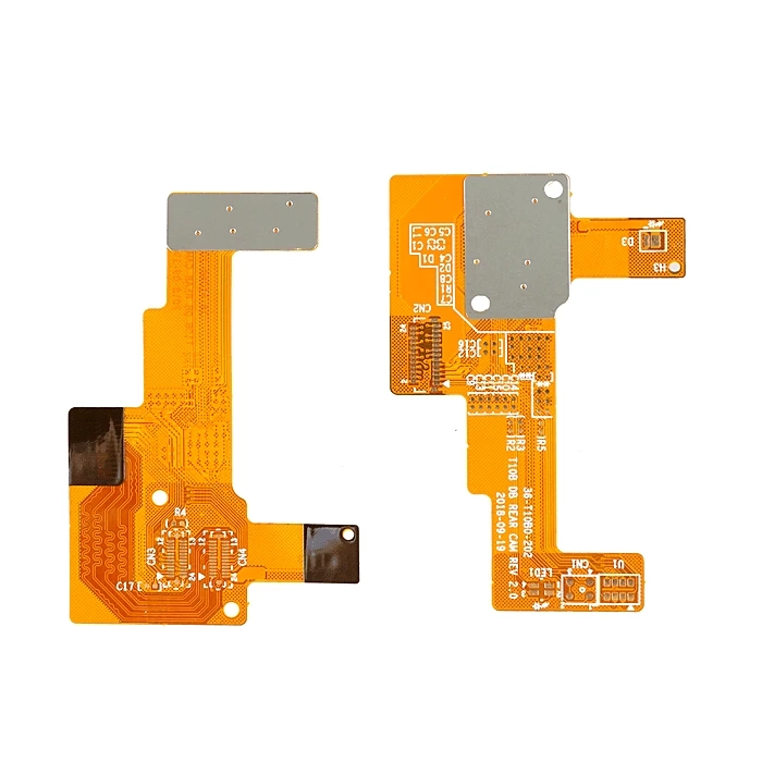
You need to first identify what you exactly desire from the prototypes. Then gather essential information. Once ready, you may start your prototyping process. You may contact a well-established PCB company to derive adequate support with the process. The company chosen should provide helpful resources and responsive customer service. This way, you can be ensured of a smooth process.
Know the different steps
- Design: It is considered to be the first stage to create a prototype PCB. You may choose any PCB design software for developing your design or contact the Top PCB Manufacturers.
- Schematic design: It describes clearly crucial information to be used by engineers and manufacturers while carrying out the production process. It tends to include information concerning hardware, components and materials used to determine and produce the board’s function. It also involves its features and component placement. Schematic design helps run effectively design rule checks.
- Routing design: Routing needs to be designed by way of traces. It is used for connecting each PCB element. When planning routing, different factors come into effect like noise sensitivity, signal noise generation and power levels.
- Bill of Materials (BOM): It contains the lists all materials and components in details that are required for production. The manufacturer will rely upon this document to obtain the correct parts. It includes vital information about each component like reference designators, quantity, footprint, value and manufacturer part number.
- Checks: Customize Flex PCB enables regularly checking throughout the process to identify functionality issues. This is crucial before moving to fabrication stage. Every aspect related to the design should be checked for potential problems.
- Printing inner layers: Copper is pre-bonded to substrate after which photoresist layer is applied. The latter hardens once exposed to UV light. Unhardened photoresist is removed.
- Creating photo film: Use provided design. The professionals will first develop the PCB’s photo film using printer referred to as a plotter for every layer. Then the board’s mask is soldered. The film created is plastic sheet that has the board’s photo negative marking those conductive and non-conductive parts.
- Layer alignment: Multiple layers will require proper alignment and accurate punching of registration holes. Perfect lining will be crucial to ensure correct inner layers after combining the layers.
Complying with the different stages
There are involved different stages in PCB prototyping phases that you should be aware of. All these stages ensure that the end results derived are more than satisfactory. It will be necessary to follow all the stages, thereby to get better results.


