


What is photolithography in nanotechnology? Photolithography, also known as electron beam lithography (EBL), uses an electron beam to draw lines on a surface. EBL can be used with anymaterial, and it’s most often used for semiconductor devices because the process leverages silicon oxide wafers.
[caption class="snax-figure" align="aligncenter" width="662"]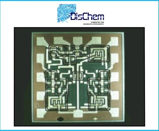 [/caption]
Electron beam lithography Charge dissipation agents are added to prevent static electricity from negatively impacting the process or damaging components. The use of photolithography in nanotechnology helps to create micro and nanoscale devices. For example, the process is commonly used to produce integrated circuits, flat panel displays, and photonic crystals. In this blog post, we will explore some common nanolithography technique application works.
How Does Nanolithography Work?
There are many different ways to perform nanolithography machining, depending on the type of material being worked with and what kind of structures will be made. Most techniques use light or electron beams for patterning in a substrate where they can protect certain areas from exposure by adding masks that have been coated with photoresists during production processes. It etches away at unwanted materials until only desired patterns remain intact before removing these protective coverings so all original features may become visible once complete.
Photolithography in Nanotechnology: How it Works
Photolithography techniques as applied to nanolithography are very similar to conventional lithography for images and printing. First, a substrate material is coated with a chemical known as a photoresist. Next, by using a mask to expose the resist to light selectively, the exposed areas harden. Next, the soft areas are etched away through a chemical process, and the procedure is repeated to build up a series of layers.
Nanolithography Technique Application
Nanolithography is a fascinating process that allows us to control material on an incredibly small scale. Its applications are impressive and have allowed us to create new technologies never before imagined. Below are some areas where the nanolithography technique has been applied:
Structural elements and functional surfaces:cantilevers for MEMS and probe tips, micro-implants, nano-tweezers, surfaces with specific hydrophobicity/hydrophilicity properties, etc.
Optical devices and elements: displays panels and masks for photosensitive materials like liquid crystals, used in various applications such as computer monitors or television sets.
Superconducting devices: arrays with Josephson junctions to enable quantum computing, high-frequency electronics, single-photon detectors, x-ray detections, etc.
Devices and energy storage or conversion elements include solar cells, batteries, energy harvesting devices, etc.
Advanced imaging is possible through nanofabrication: TEM lamellae preparation and 3D FIB-SEM imaging. Atom probe tomography is another example.
Final Thoughts
We have provided you with some insight into how photolithography in nanotechnology works and the benefits it may provide. Photolithographic processes are used to create an image with high resolution and accuracy without using materials that may be toxic or difficult to work with.