


Since 1958, nanolithography techniques have grown within nanotechnology, dealing with the engineering structures such as writing, etching, and printing the nanometer scale. This growth evolved to cover the design of structures either in the nanometer range or within the range of 10-9 or 10-6 meters.
However, the nanolithography field, which is a part of lithography, covers smaller structures separated into two techniques. That\'s those that directly write the desired structures to a surface and those that etch away molecules, leaving behind the desired structure
But, you probably might be wondering, what has photolithography got to do with nanotechnology. Well, this article covers that. Keep reading further as we unravel the connection between photolithography and nanotechnology. Shall we?
What is Photolithography?
Before we delve fully into what photolithography is and its connection with nanotechnology, let\'s talk a bit about Nanolithography as it may help you understand this entire concept.
In simple terms, Nanolithography is a technique that produces nanoscale structures through a mold with 3D surface designs. It\'s done by placing your 3D designs against a very heated cast.
This technology has been used for years to manufacture integrated circuits and creates patterns with the size of a nanometer range.
On the other hand, photolithography creates a pattern for a slice on the surface of a device material. To produce an electronic device, a few stages of photolithography is required. And they are gradually using such patterns to create etched areas or metal contact.
How does photolithography affect nanotechnology
Before the evolution of the semiconductor industry, chemical structures were produced and represented in large scales making it difficult to comprehend.
However, during the transition (that\'s while the industry\'s evolution began), the demand for techniques capable of producing micro and nanoscale structures shot up.
In that growth process, photolithography was applied initially to the available structures in 1958 and reproduced in smaller nanometer scales ever since it has become the most "commercially successful technique" capable of reproducing in sub-100 nanometer patterns.
Although, several other techniques are connected with this field. However, each technique serves its users in the semiconductor, technology, and medical industries alike.
Eventually, breaking these structures contributes a great deal to the advancement of nanotechnology, making it very important in our world today as there\'s an increase in the demand for smaller chips.
Nanotechnology Companies
Nanotechnology is being practiced in several countries and companies around the world. A few companies that offer nanotechnology services in the U.S are:
10 Angstroms
3D systems
4 wave
A & A company
Abeam technologies but to mention a few
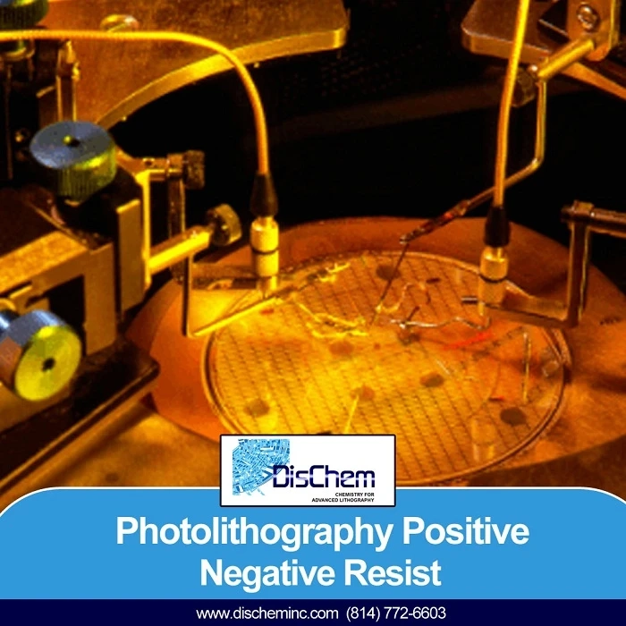
But as you\'ve known, photolithography plays a huge role in nanotechnology. So, if you need photolithography services, Dischem chemicals can be your go-to as they offer amazing lithography services. Whether photolithography or Nanolithography.
Conclusion
When in need of chemical-related services, look no further than Dischem chemicals. With our years of experience and knowledge in this industry, rest assured you\'ll get whatever chemical you may need for your experiences. Contact us today for any products and services you may need, and thank me later.